×

Applied Materials WSJ Piece

Applied Materials Inc. Chief Executive Gary Dickerson spent 18 months promoting an acquisition that would have created a $29 billion technology giant, only to be foiled by the U.S. Justice Department’s antitrust division. Now he has to sell another plan, one that exploits some major changes affecting makers of computer chips.

His Silicon Valley company, which makes machines that help churn out the silicon brains of devices from smartphones to supercomputers, is using an industry trade show this week to try to persuade analysts that Applied will be just as well off without merging with fellow tool-maker Tokyo Electron Ltd. His plan rests in part on an assumption that the 48-year-old firm’s new production systems, which are being unveiled Monday at the Semicon West trade show in San Francisco, can grab market share from rival sellers of chip-making equipment.

This strategy underscores broader issues in the market for chips, which are fabricated using multimillion-dollar machines that process plate-sized silicon wafers. Progress in the industry has been driven for 50 years by shrinking the size of transistors and other circuitry, allowing manufacturers to pack more features on chips at a lower cost. But miniaturization alone isn’t boosting computing performance at the rate it once did, and lately some companies haven’t been able to reduce per-transistor costs as in the past.

“What keeps customers up at night are these inflection points,” Mr. Dickerson said. “For them it’s really life or death.”

So chip makers are trying new ways to boost the speed and data-storage capacity of their products, using techniques that Mr. Dickerson believes play to the strengths of Applied’s tools.

Growth may not come easily. Many manufacturers, including giant Intel Corp., are trying to cut back on equipment purchases amid weak demand for products like personal computers, which rely on the latest chips.

Researchers at Gartner Inc. plan to release a new forecast this week for spending on wafer-processing equipment in 2015, putting sales roughly flat at $33.7 billion. That’s a downward revision from a forecast in April of 5% growth, and it was caused by currency-exchange issues affecting big tool makers in Europe and Asia. Gartner expects the market to decline 3.5% in 2016.

Applied, the biggest maker of such equipment, has tried to minimize the effects of the industry’s cycles by adding gear to make liquid-crystal displays and solar panels. Its boldest bid to grow faster than the market was a $9.3 billion stock-swap deal for Tokyo Electron announced in September 2013, the same month Mr. Dickerson assumed the CEO position.

Acquiring that company—which was No. 3 in the market by revenue—would have given Applied both entirely new machines and similar systems for different stages of chip making, Mr. Dickerson said. He went so far as to move his family to Tokyo to prepare to lead the combined firms.

But Justice Department officials, after a lengthy investigation, concluded the combination would reduce competition to develop future tools. Applied abandoned the deal in late April; its shares fell 8% on the day of the announcement, and they are off 25% since the start of the year.

Romit Shah, an analyst at Nomura Securities, said that investors who bought Applied shares because of the merger potential are gradually selling their positions. Current stockholders are waiting for what Mr. Dickerson and other Applied executives may disclose at a meeting with analysts Monday afternoon, he said, including potential revenue targets and cost-cutting moves.

One of the biggest changes Mr. Dickerson is trying to exploit involves the transistors used in microprocessors, which provide calculating power to digital devices. Manufacturers have been racing to follow Intel’s lead in creating a new breed of transistors with fin-like shapes that switch off and on faster.

Meanwhile, makers of the chips called NAND flash memory, used to store data in portable devices, fear the chips will become unreliable if circuitry gets much smaller. So they plan to boost data-storage capacity by stacking relatively large transistors in 32-to-64 layers.

These changes, analysts say, favor companies that make tools that add or subtract materials on wafers. One particular focus is etching, the process of removing silicon and other materials for purposes such as shaping transistors and cutting grooves for microscopic wiring on chips.

Lam Research Corp. leads the market for etching equipment, a field where Applied long struggled, said Dan Hutcheson, an analyst at VLSI Research. But he estimated that Applied’s market share in etching has risen from 11% in the 2012 first quarter to 21% in this year’s like period. VLSI said Lam’s share declined to 41% from 45% over that period.

On Monday, Applied expects to formally introduce an etching machine called Centris Sym3 to help accelerate its market-share push. Early sales indicate the system, which has already begun shipping to customers, “is the fastest-ramping product in the history of Applied,” Mr. Dickerson said. The company is also introducing a new system for a process called atomic layer deposition.

Lam doesn’t sound worried. Doug Bettinger, its executive vice president and chief financial officer, insists that its market share has grown in the past two years, and he said his company would also benefit from the technology trends Applied hopes to capitalize on. Lam has scheduled its own analyst meeting Tuesday at Semicon West.

“Customers come to us with their biggest etching challenges,” Mr. Bettinger said.

sri 10 years ago
×

samsung's 2250ppi display coming??

Samsung Develops ‘11K’ Super-Resolution Display Along With 13 Companies…Putting 26.5 Mil USD For 5Years Jul 10, 2015

Samsung Display is planning to develop world’s first 11K super-resolution display by working together with industry and education. Government is investing 26.5 million dollars by stages for 5 years hereafter. At 10th Display Field National Research Development Business General Workshop that was held at Muju Deogyusan Resort, Executive Director Chu Hye Yong of Samsung Display’s Base Technology Department said that it is challenging itself to develop super-resolution display with 2250 ppi, which is number of pixels per inch that is 3 times higher than previous resolution, and started development process with 13 domestic and foreign companies starting from the 1st of June. Executive Director Chu Hye Yong of Samsung Display’s Base Technology Department is holding a keynote lecture at 10th Display Field National Research Development Business General Workshop that was held at Muju Deogyusan Resort.

This business is part of GiGA Korea’s business that is being led by Ministry of Science, ICT, and Future Planning (MSIP), and name of the project is EnDK. It is predicted that prototype can be shown to the public at 2018 Pyeongchang Winter Olympics at the earliest. As a main company that is overseeing the project, Samsung Display is aiming for a goal that allows 2250 ppi-level 11K display for mobiles to implement 3D-effect. If display panel’s resolution increases extremely, there is an optical illusion where it is same as watching 3D screen. Because 11K is able to show screen colors in detail, it is able to show 3D-effect. Currently 500 ppi-level 2K (2560x1440) display product is being released as one with the best specification in mobile display field. A prototype with 8K resolution came out in large-sized display for TVs field, and most of UHD 4K products are considered as the ones with best resolution. “We are hoping that we are able to show such technologies at Pyeongchang Olympics if there is a progress in developing technologies. Although some might think that 11K as ‘over specification’ that consumers do not need, this can work as a basis for Korean display industry take another leap if related materials and parts improve through this.” Executive Director Chu stressed the importance of this technology for the future.

Staff Reporter Sung, Hyeonhee | sunghh@etnews.com

sri 10 years ago
×

iphone cost analysis

sri 9 years ago
×

Low yields, high costs with LTPS

China makers share different views on OLED TV development, says report

Amy Fan, Taipei; Alex Wolfgram, DIGITIMES [Tuesday 21 July 2015]

According to chairman Zhou Houjian of China vendor Hisense, Korea panel makers' development of OLED TV panels potentially poses a threat for China makers in the long term but over the next five years the technology will not have a competitive edge in the market due to low yields and high costs, according to a new report from ZDNet Korea.

TCL representatives, however, were quoted in the report as stating they believe LCD panels have an advantage over OLED, as OLED is expected to suffer from color loss after five years of use and has a short lifespan.

LG Electronics' OLED TV sales reached 15,000 during the first half of 2015 as a result of high pricing and China TV makers are currently rethinking their strategies for OLED TV production in the future, the report said.

Despite these trends, LG is pushing investments into OLED TV panel production while other panel makers believe Quantum Dot (QD) and wide color gamut (WCG) Ultra HD (4K) TVs will have a higher acceptance in the market.

China and Taiwan panel makers meanwhile are investing in OLED, but mainly for small- to medium-size panels.

sri 10 years ago
×

TANGENT!

sri 9 years ago
×

Samsung OLED investments

May 7 2015 by OLEDNET

Due to the shortage in supply of Galaxy S6 Edge from its higher than expected demand, Samsung Display’s worry regarding flexible AMOLED line investment is deepening.

Samsung Electronics’ announced target sales for Galaxy S6 and S6 Edge is 70,000,000 units. If the S6 Edge sales occupies approximately 40%, it is estimated that about 28,000,000 units of S6 Edge will be sold.

Samsung Display’s A2 and A3 lines can produce flexible AMOLED panel that is currently used for S6 Edge. Considering the yield and operation rate, it is analyzed that approximately 5,000,000 units can be produced from A2 in a quarter, and 7,000,000 units from A3 (A2 line = 15K, A3 line = 15K). However, as only A2 was in operation in 1Q, assuming that about 5,000,000 units were supplied, and that A3 will also be operational from 2Q, it is forecast that approximately 12,000,000 units will be supplied. Therefore, it is estimated that A2 and A3 lines have to be in full operation until 3Q to meet the demand for S6 Edge.

However, if flexible AMOLED panel is applied to the new Galaxy Note model in 4Q, the preparation for mass production needs to begin from 3Q. Hence, with the current Samsung Display’s flexible mass production capa., it looks to be difficult to meet the demand for flexible AMOLED panel. Consequently, Samsung’s additional flexible AMOLED line expansion seems unavoidable.

To establish additional capa. Samsung Display could consider replacement investment for A2 line, or expanding the A3 line. If A2 line is replacement invested, the investment cost would decrease and move up the mass production schedule. Nevertheless, the fall in the total market share has to be considered following the reduced rigid panel supply from diminished capa. of rigid AMOLED panel. If A3 line is expanded, the investment cost and time required will be higher but considering future supply to other set companies that are not Samsung Electronics, this is analyzed to be more advantageous compared to the replacement investment for A2 line.

As a result, the industry’s attention is focused on how Samsung Display will choose between A2 line and A3 line, or if both will be carried out.

By DaRae Kim, reporter@olednet.co.kr

sri 10 years ago
×

GOAL

Get Dad's startup funded.

sri 10 years ago
×

ARCTANGENT!

sri 10 years ago
×

TANGENT!

sri 9 years ago
×

China goes OLED crazy

China makers' production capacity for small- to medium-size AMOLED panels is expected to increase 373% in 2017 compared with what it is in 2015 as makers continue to invest in new facilities and capacity expansion, according to Digitimes Research.

As of 2014 Taiwan makers held a larger production capacity over China makers but as investments and expanded production at 6G and below facilities continue from China makers, their production capacity will spike 373% to give them the global number two spot behind Korea makers in terms of overall small- to medium-size AMOLED capacity.

In Taiwan, AU Optronics (AUO) currently has the strongest position in developing AMOLED panels, and the company has a base in Singapore with some of the latest equipment, giving the company strong yields.

In China, BOE is pushing forth investments into small- to medium-size AMOLED panels in addition to OLED TV panels, while China Star Optoelectronics Technology (CSOT) will allocate 6G facilities in Wuhan for small- to medium-size LTPS TFT LCD and AMOLED displays.

Tianma Microelectronics, Everdisplay (EDO) and GoVisionox (GVO) are also investing in AMOLED facilities, said Digitimes Research. Additionally, Truly Optoelectronics is expected to purchase old 4.5G AMOLED production facilities from Samsung Display, giving the company a total of 10 lines for small-, medium- and large-size AMOLED panels.

sri 10 years ago
×

iphone teardown

sri 9 years ago
×

how LCDs are made

sri 9 years ago
×

how LTPS works

sri 9 years ago
×

LTPS annealing

sri 9 years ago
×

future military OLED screen?

sri 9 years ago
×

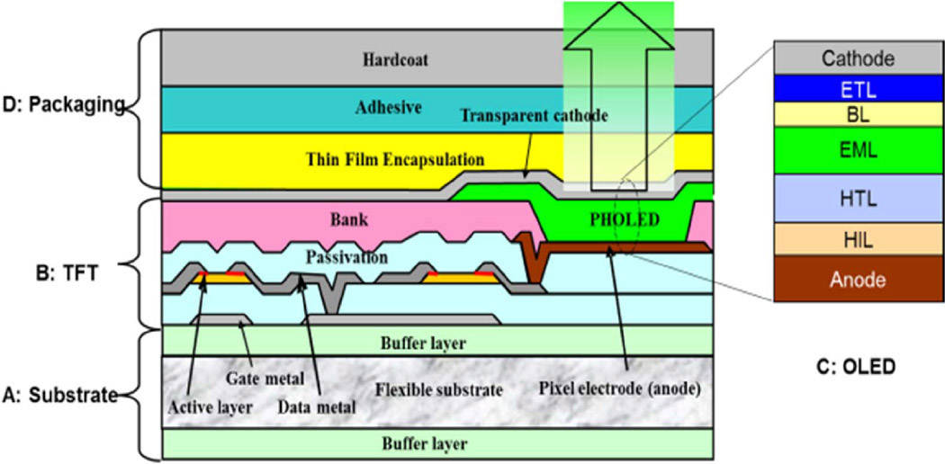
flexible oled cross section

Figure 3.The cross-section of a flexible active matrix OLED(AMOLED)display structure.BL:Blocking layer.TFT:Thin-film transistor.For the backplane technology,amorphous silicon(a-Si)TFTs have the advantages of showing uniform electrical characteristics over large areas,a reasonable field-effect mobility(∼0.5cm2/V·s),a low-temperature process(<300°C),and low-cost fabrication.4 Simple circuitry can be added to compensate for threshold-voltage instability shifts.Moreover,the low drive voltage of high-efficiency PHOLEDs further reduces these shifts.We have demonstrated a flexible AMOLED display using a-Si backplane technology.

sri 9 years ago
+